
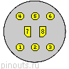
| Pin Number |
Pin Name |
Description |
| 1 | Reserve or Ready | on older systems |
| 2 | Reset | Reset signal sent to slaves. Slaves can not send resets to master. LOW going pulse signals the system reset. |
| 3 | SIRCS | decoded by master then may issue UniLink commands. This line is used by the master to receive SIRCS data (Serial InferRed Control System, also known as Control-S). |
| 4 | Clock | from master. Bus clock signal generated from the master for all bus signals. |
| 5 | Data | bidirectional 5V TTL I/O. When the bus is active it may be idle or active. When idle the bus appears as a square wave with a period of 16ms (8ms low and 8ms high). When the data bus is active and data is flowing the pulse width of the square wave will change length depending on the data word length. |
| 6 | Bus-On | from master, cascaded to other slaves. When the bus is off, it is in 'sleep' mode and there is no data communications. High=ON. Low=OFF |
| 7 | +12V Backup | +12V 2A max |
| 8 | GND |
Signals are TTL 0V (LOW) or 5V (HIGH)
 correct
 incorrect