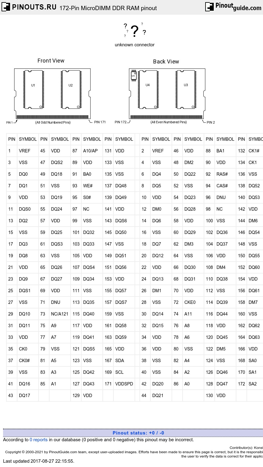

| PIN | SYMBOL | PIN | SYMBOL | PIN | SYMBOL | PIN | SYMBOL | PIN | SYMBOL | PIN | SYMBOL | PIN | SYMBOL | PIN | SYMBOL | |||||||||||||||||||||||||||||||||||||||||||||||||||||||||||||||||||
| 1 | VREF | 45 | VDD | 87 | A10/AP | 131 | VDD | 2 | VREF | 46 | VDD | 88 | BA1 | 132 | CK1# | |||||||||||||||||||||||||||||||||||||||||||||||||||||||||||||||||||
| 3 | VSS | 47 | DQS2 | 89 | VDD | 133 | VSS | 4 | VSS | 48 | DM2 | 90 | VDD | 134 | CK1 | |||||||||||||||||||||||||||||||||||||||||||||||||||||||||||||||||||
| 5 | DQ0 | 49 | DQ18 | 91 | BA0 | 135 | VSS | 6 | DQ4 | 50 | DQ22 | 92 | RAS# | 136 | VSS | |||||||||||||||||||||||||||||||||||||||||||||||||||||||||||||||||||
| 7 | DQ1 | 51 | VSS | 93 | WE# | 137 | DQ48 | 8 | DQ5 | 52 | VSS | 94 | CAS# | 138 | DQ52 | |||||||||||||||||||||||||||||||||||||||||||||||||||||||||||||||||||
| 9 | VDD | 53 | DQ19 | 95 | S0# | 139 | DQ49 | 10 | VDD | 54 | DQ23 | 96 | DNU | 140 | DQ53 | |||||||||||||||||||||||||||||||||||||||||||||||||||||||||||||||||||
| 11 | DQS0 | 55 | DQ24 | 97 | NC | 141 | VDD | 12 | DM0 | 56 | DQ28 | 98 | NC | 142 | VDD | |||||||||||||||||||||||||||||||||||||||||||||||||||||||||||||||||||
| 13 | DQ2 | 57 | VDD | 99 | VSS | 143 | DQS6 | 14 | DQ6 | 58 | VDD | 100 | VSS | 144 | DM6 | |||||||||||||||||||||||||||||||||||||||||||||||||||||||||||||||||||
| 15 | VSS | 59 | DQ25 | 101 | DQ32 | 145 | DQ50 | 16 | VSS | 60 | DQ29 | 102 | DQ36 | 146 | DQ54 | |||||||||||||||||||||||||||||||||||||||||||||||||||||||||||||||||||
| 17 | DQ3 | 61 | DQS3 | 103 | DQ33 | 147 | VSS | 18 | DQ7 | 62 | DM3 | 104 | DQ37 | 148 | VSS | |||||||||||||||||||||||||||||||||||||||||||||||||||||||||||||||||||
| 19 | DQ8 | 63 | VSS | 105 | VDD | 149 | DQ51 | 20 | DQ12 | 64 | VSS | 106 | VDD | 150 | DQ55 | |||||||||||||||||||||||||||||||||||||||||||||||||||||||||||||||||||
| 21 | VDD | 65 | DQ26 | 107 | DQS4 | 151 | DQ56 | 22 | VDD | 66 | DQ30 | 108 | DM4 | 152 | DQ60 | |||||||||||||||||||||||||||||||||||||||||||||||||||||||||||||||||||
| 23 | DQ9 | 67 | DQ27 | 109 | DQ34 | 153 | VDD | 24 | DQ13 | 68 | DQ31 | 110 | DQ38 | 154 | VDD | |||||||||||||||||||||||||||||||||||||||||||||||||||||||||||||||||||
| 25 | DQS1 | 69 | VDD | 111 | VSS | 155 | DQ57 | 26 | DM1 | 70 | VDD | 112 | VSS | 156 | DQ61 | |||||||||||||||||||||||||||||||||||||||||||||||||||||||||||||||||||
| 27 | VSS | 71 | DNU | 113 | DQ35 | 157 | DQS7 | 28 | VSS | 72 | CKE0 | 114 | DQ39 | 158 | DM7 | |||||||||||||||||||||||||||||||||||||||||||||||||||||||||||||||||||
| 29 | DQ10 | 73 | NC/A121 | 115 | DQ40 | 159 | VSS | 30 | DQ14 | 74 | A11 | 116 | DQ44 | 160 | VSS | |||||||||||||||||||||||||||||||||||||||||||||||||||||||||||||||||||
| 31 | DQ11 | 75 | A9 | 117 | VDD | 161 | DQ58 | 32 | DQ15 | 76 | A8 | 118 | VDD | 162 | DQ62 | |||||||||||||||||||||||||||||||||||||||||||||||||||||||||||||||||||
| 33 | VDD | 77 | A7 | 119 | DQ41 | 163 | DQ59 | 34 | VDD | 78 | A6 | 120 | DQ45 | 164 | DQ63 | |||||||||||||||||||||||||||||||||||||||||||||||||||||||||||||||||||
| 35 | CK0 | 79 | VSS | 121 | DQS5 | 165 | VDD | 36 | VDD | 80 | VSS | 122 | DM5 | 166 | VDD | |||||||||||||||||||||||||||||||||||||||||||||||||||||||||||||||||||
| 37 | CK0# | 81 | A5 | 123 | VSS | 167 | SDA | 38 | VSS | 82 | A4 | 124 | VSS | 168 | SA0 | |||||||||||||||||||||||||||||||||||||||||||||||||||||||||||||||||||
| 39 | VSS | 83 | A3 | 125 | DQ42 | 169 | SCL | 40 | VSS | 84 | A2 | 126 | DQ46 | 170 | SA1 | |||||||||||||||||||||||||||||||||||||||||||||||||||||||||||||||||||
| 41 | DQ16 | 85 | A1 | 127 | DQ43 | 171 | VDDSPD | 42 | DQ20 | 86 | A0 | 128 | DQ47 | 172 | SA2 | |||||||||||||||||||||||||||||||||||||||||||||||||||||||||||||||||||
| 43 | DQ17 | 129 | VDD | 44 | DQ21 | 130 | VDD | |||||||||||||||||||||||||||||||||||||||||||||||||||||||||||||||||||||||||||
NOTE: Pin 73 is NC for the 64MB module. It is A12 for the 128MB and 256MB modules.
Pin Descriptions
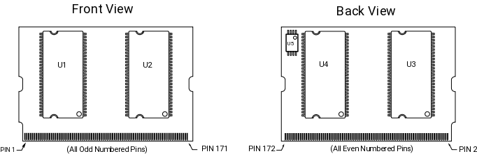
Pin numbers may not correlate with symbols; refer to Pin Assignment tables on page 3 for more information
| PIN NUMBERS | SYMBOL | TYPE | DESCRIPTION | |||||||||||||||||||||||||||||||||||||||||||||||||||||||||||||||||||||||||||||
| 92, 93, 94 | WE#, CAS#, RAS# | Input | Command Inputs: RAS#, CAS#, and WE# (along with S#) define the command being entered. | |||||||||||||||||||||||||||||||||||||||||||||||||||||||||||||||||||||||||||||
| 35, 37, 132, 134 | CK0, CK0# CK1, CK1# | Input | Clock: CK and CK# are differential clock inputs. All address and control input signals are sampled on the crossing of the positive edge of CK and negative edge of CK#. Output data (DQs and DQS) is refer- enced to the crossings of CK and CK#. | |||||||||||||||||||||||||||||||||||||||||||||||||||||||||||||||||||||||||||||
| 72 | CKE0 | Input | Clock Enable: CKE HIGH activates and CKE LOW deactivates the internal clock, input buffers, and output drivers. Taking CKE LOW provides PRECHARGE POWER-DOWN and SELF REFRESH operations (all device banks idle), or ACTIVE POWER-DOWN (row ACTIVE in any device bank). CKE is synchronous for POWER-DOWN entry and exit, and for SELF REFRESH entry. CKE is asynchronous for SELF REFRESH exit and for disabling the outputs. CKE must be maintained HIGH throughout read and write accesses. Input buffers (excluding CK, CK# and CKE) are disabled during POWER-DOWN. Input buffers (excluding CKE) are disabled during SELF REFRESH. CKE is an SSTL_2 input but will detect an LVCMOS LOW level after VDD is applied and until CKE is first brought HIGH. After CKE is brought HIGH, it becomes an SSTL_2 input only. |
|||||||||||||||||||||||||||||||||||||||||||||||||||||||||||||||||||||||||||||
| 95 | S0# | Input | Chip Select: S# enables (registered LOW) and disables (registered HIGH) the command decoder. All commands are masked when S# is registered HIGH. S# is considered part of the command code. | |||||||||||||||||||||||||||||||||||||||||||||||||||||||||||||||||||||||||||||
| 88, 91 | BA0, BA1 | Input | Bank Address: BA0 and BA1 define to which device bank an ACTIVE, READ, WRITE, or PRECHARGE command is being applied. | |||||||||||||||||||||||||||||||||||||||||||||||||||||||||||||||||||||||||||||
| 73 (128MB, 256MB), 75, 77, | A0–A11 | Input | Address Inputs: A0-A11/A12 provide the row address for | |||||||||||||||||||||||||||||||||||||||||||||||||||||||||||||||||||||||||||||
| 81, 83, 85, 87, 74, 76, 78, 82, | (64MB) | ACTIVE commands, and the column address and auto | ||||||||||||||||||||||||||||||||||||||||||||||||||||||||||||||||||||||||||||||
| 84, 86 | A0–A12 | precharge bit (A10) for READ/WRITE commands, to select | ||||||||||||||||||||||||||||||||||||||||||||||||||||||||||||||||||||||||||||||
| (128MB, 256MB) | one location out of the memory array in the respective | |||||||||||||||||||||||||||||||||||||||||||||||||||||||||||||||||||||||||||||||
| device bank. A10 sampled during a PRECHARGE command | ||||||||||||||||||||||||||||||||||||||||||||||||||||||||||||||||||||||||||||||||
| determines whether the PRECHARGE applies to one device | ||||||||||||||||||||||||||||||||||||||||||||||||||||||||||||||||||||||||||||||||
| bank (A10 LOW, device bank selected by BA0, BA1) or all | ||||||||||||||||||||||||||||||||||||||||||||||||||||||||||||||||||||||||||||||||
| device banks (A10 HIGH). The address inputs also provide the | ||||||||||||||||||||||||||||||||||||||||||||||||||||||||||||||||||||||||||||||||
| op-code during a MODE REGISTER SET command. BA0 and | ||||||||||||||||||||||||||||||||||||||||||||||||||||||||||||||||||||||||||||||||
| BA1 define which mode register (mode register or extended | ||||||||||||||||||||||||||||||||||||||||||||||||||||||||||||||||||||||||||||||||
| mode register) is loaded during the LOAD MODE REGISTER | ||||||||||||||||||||||||||||||||||||||||||||||||||||||||||||||||||||||||||||||||
| command. | ||||||||||||||||||||||||||||||||||||||||||||||||||||||||||||||||||||||||||||||||
| 12, 26, 48, 62, 108, 122, 144, 158 |
DM0–DM7 | Input | Data Mask: DM is an input mask signal for write data. Input data is masked when DM is sampled HIGH along with that input data during a WRITE access. DM is sampled on both edges of DQS. Although DM pins are input-only, the DM loading is designed to match that of DQ and DQS pins. | |||||||||||||||||||||||||||||||||||||||||||||||||||||||||||||||||||||||||||||
| 1, 2 | VREF | Input | SSTL_2 reference voltage. | |||||||||||||||||||||||||||||||||||||||||||||||||||||||||||||||||||||||||||||
| 167 | SDA | Input/ Output | Serial Presence-Detect Data: SDA is a bidirectional pin used to transfer addresses and data into and out of the presence- detect portion of the module. | |||||||||||||||||||||||||||||||||||||||||||||||||||||||||||||||||||||||||||||
| 169 | SCL | Input | Serial Clock for Presence-Detect: SCL is used to synchronize the presence-detect data transfer to and from the module. | |||||||||||||||||||||||||||||||||||||||||||||||||||||||||||||||||||||||||||||
| 168, 170, 172 | SA0–SA2 | Input | Presence-Detect Address Inputs: These pins are used to configure the presence-detect device. | |||||||||||||||||||||||||||||||||||||||||||||||||||||||||||||||||||||||||||||
| 11, 25, 47, 61, 107, 121, 143, 157 |
DQS0-DQS7 | Input/ Output | Data Strobe: Output with READ data, input with WRITE data. DQS is edge-aligned with READ data, centered in WRITE data. Used to capture data. | |||||||||||||||||||||||||||||||||||||||||||||||||||||||||||||||||||||||||||||
| 5, 7, 13, 17, 19, 23, 29, 31 41, 43, 49, 53, 55, 59, 65, 67, 101, 103, 109, 113, 115, 119, 125, 127, 137, 139, 145, 149, 151, 155, 161, 163, 6, 8, 14, 18, 20, 24, 30, 32, 42, 44, 50, 54, 56, 60, 66, 68, 102, 104, 110, 114, 116, 120, 126, 128, 138, 140, 146, 150, 152, 156, 162, 164 |
DQ0-DQ63 | Input/ Output | Data I/Os: Data bus. | |||||||||||||||||||||||||||||||||||||||||||||||||||||||||||||||||||||||||||||
| 9, 21, 33, 45, 57, 69, 89, 105, 117, 129, 131, 141, 153, 165, 10, 22, 34, 36, 46, 58, 90, 106, 118, 130 142, 154, 166 |
VDD | Supply | DQ Power Supply: +2.5V ±0.2V. | |||||||||||||||||||||||||||||||||||||||||||||||||||||||||||||||||||||||||||||
| 3, 15, 27, 39, 51, 63, 99, 111, 123, 133, 135, 147, 159, 4, 16, 28, 38,40, 52, 64, 100, 112, 124, 136, 148, 160 |
VSS | Supply | Ground: +2.3V to +3.6V. | |||||||||||||||||||||||||||||||||||||||||||||||||||||||||||||||||||||||||||||
| 171 | VDDSPD | Supply | Serial EEPROM positive power supply. | |||||||||||||||||||||||||||||||||||||||||||||||||||||||||||||||||||||||||||||
| 73 (64MB), 97, 98 | NC | – | No Connect: These pins should be left unconnected. | |||||||||||||||||||||||||||||||||||||||||||||||||||||||||||||||||||||||||||||
| 71, 96 | DNU | – | Do Not Use: These pins are not connected on this module but are assigned pins on other modules in this product family. | |||||||||||||||||||||||||||||||||||||||||||||||||||||||||||||||||||||||||||||
 correct
 incorrect