- Reduced form-factor to 90 by 96 mm.
- Eliminated the need for backplanes or card cages, through its self-stacking bus
- Minimized component count and power consumption (to typically 1-2 Watts per module), by reducing required bus drive on most signals to 4 mA.
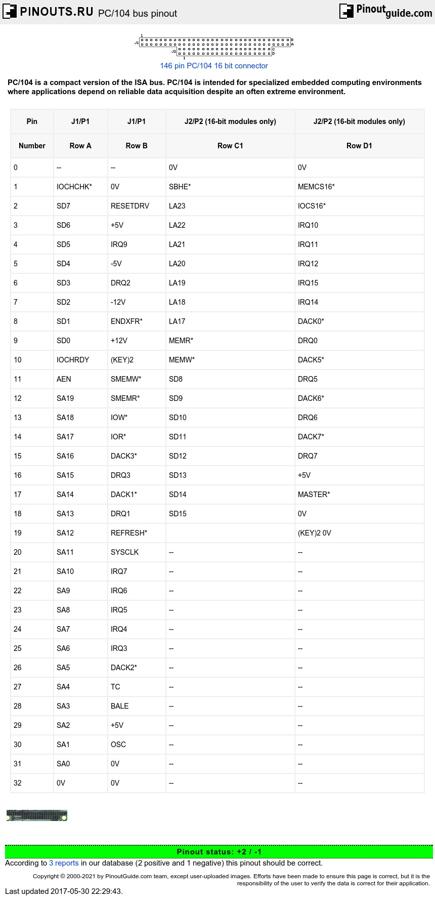
PC/104 modules can be of two bus types, 8-bit and 16-bit. These correspond to the PC and PC/AT buses, respectively.
| Pin | J1/P1 | J1/P1 | J2/P2 (16-bit modules only) | J2/P2 (16-bit modules only) |
|---|---|---|---|---|
| Number | Row A | Row B | Row C1 | Row D1 |
| 0 | -- | -- | 0V | 0V |
| 1 | IOCHCHK* | 0V | SBHE* | MEMCS16* |
| 2 | SD7 | RESETDRV | LA23 | IOCS16* |
| 3 | SD6 | +5V | LA22 | IRQ10 |
| 4 | SD5 | IRQ9 | LA21 | IRQ11 |
| 5 | SD4 | -5V | LA20 | IRQ12 |
| 6 | SD3 | DRQ2 | LA19 | IRQ15 |
| 7 | SD2 | -12V | LA18 | IRQ14 |
| 8 | SD1 | ENDXFR* | LA17 | DACK0* |
| 9 | SD0 | +12V | MEMR* | DRQ0 |
| 10 | IOCHRDY | (KEY)2 | MEMW* | DACK5* |
| 11 | AEN | SMEMW* | SD8 | DRQ5 |
| 12 | SA19 | SMEMR* | SD9 | DACK6* |
| 13 | SA18 | IOW* | SD10 | DRQ6 |
| 14 | SA17 | IOR* | SD11 | DACK7* |
| 15 | SA16 | DACK3* | SD12 | DRQ7 |
| 16 | SA15 | DRQ3 | SD13 | +5V |
| 17 | SA14 | DACK1* | SD14 | MASTER* |
| 18 | SA13 | DRQ1 | SD15 | 0V |
| 19 | SA12 | REFRESH* | (KEY)2 0V | |
| 20 | SA11 | SYSCLK | -- | -- |
| 21 | SA10 | IRQ7 | -- | -- |
| 22 | SA9 | IRQ6 | -- | -- |
| 23 | SA8 | IRQ5 | -- | -- |
| 24 | SA7 | IRQ4 | -- | -- |
| 25 | SA6 | IRQ3 | -- | -- |
| 26 | SA5 | DACK2* | -- | -- |
| 27 | SA4 | TC | -- | -- |
| 28 | SA3 | BALE | -- | -- |
| 29 | SA2 | +5V | -- | -- |
| 30 | SA1 | OSC | -- | -- |
| 31 | SA0 | 0V | -- | -- |
| 32 | 0V | 0V | -- | -- |
Rows C and D are not required on 8-bit modules. B10 and C19 are key locations.
Signal timing and function are as specified in ISA specification. Signal source/sink current differ from ISA values.


 correct
 incorrect