

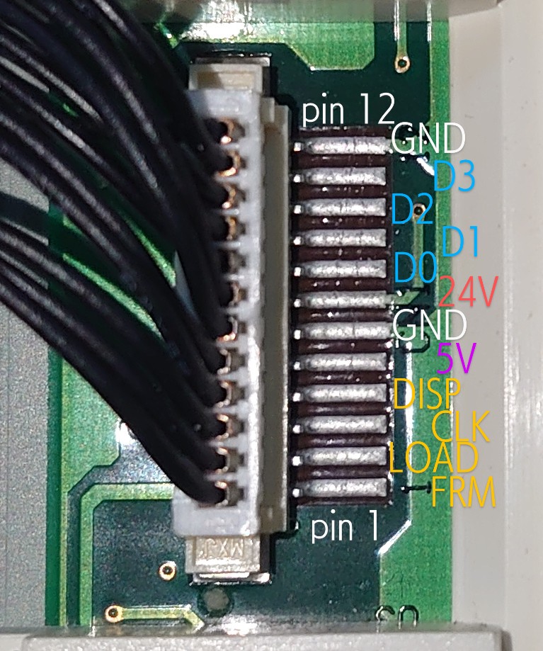
| Pin Number |
Pin Name |
Description |
|---|---|---|
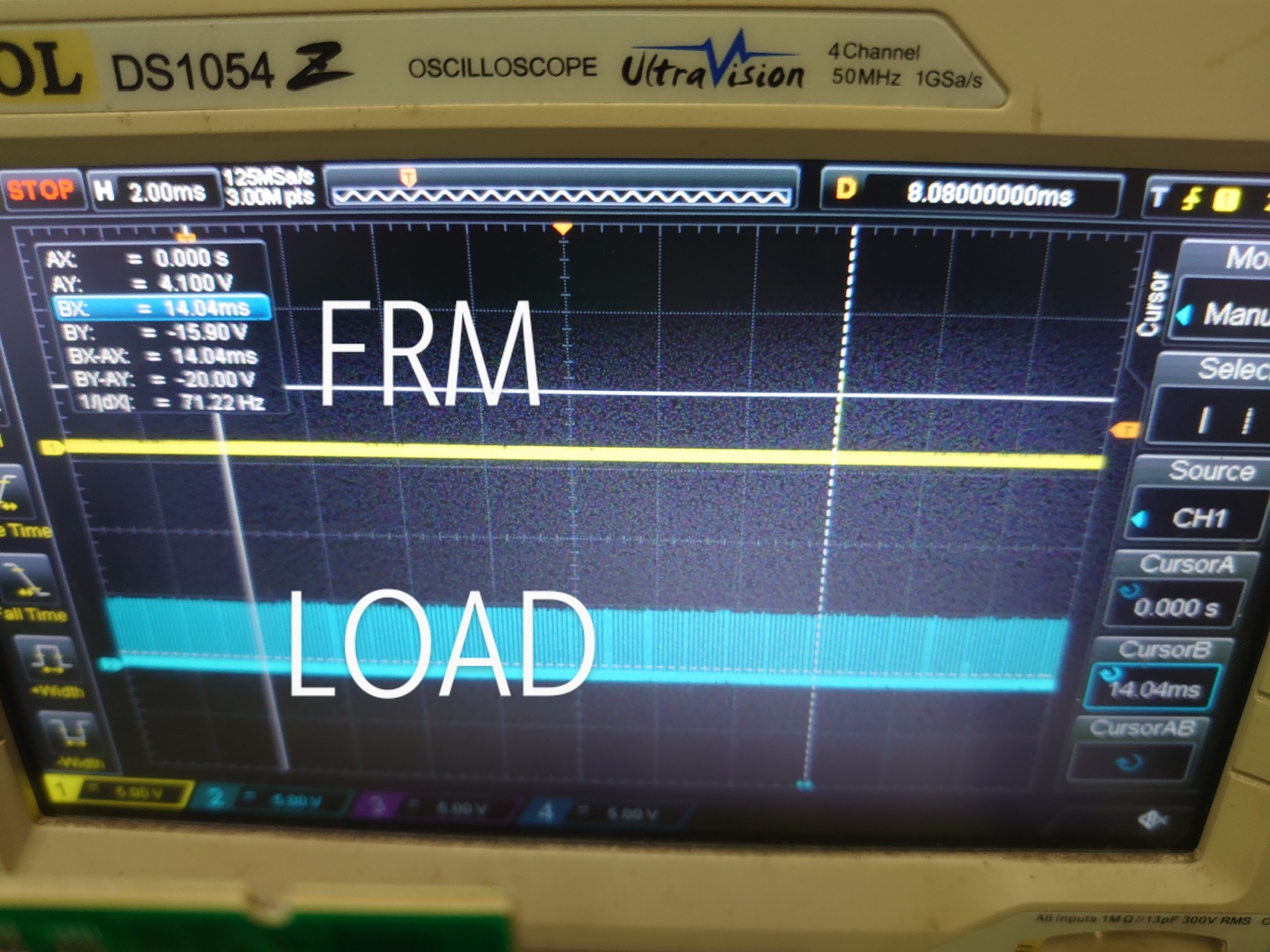
| 1 | FRM | Frame strobing pin, goes high on first row (line) data |
| 2 | LOAD | Data latching pin, goes low when writing each line data. Behaving more like a horizontal sync signal |
| 3 | CLK (or CP) | Data clocking pin, Display data made available by MPU on rising edge, sample by display on falling edge |
| 4 | DISP | Display enable pin, Active high |
| 5 | VDD | 5 VDC digital logic supply |
| 6 | GND | Ground pin |
| 7 | VEE | 24 VDC LCD bias voltage (Vary from 21 VDC to 24 VDC depends on display contrast setting) |
| 8 | D0 | Bit 0 pixel data input |
| 9 | D1 | Bit 1 pixel data input |
| 10 | D2 | Bit 2 pixel data input |
| 11 | D3 | Bit 3 pixel data input |
| 12 | GND | Ground pin |
The connector type is Molex Wire to board connector call Picoblade. This one has 12 pins and 1.25mm pin pitch.
There's chinese-made conpatible connector from SHOU HAN that you can source from LCSC.
Extra useful information of this display :
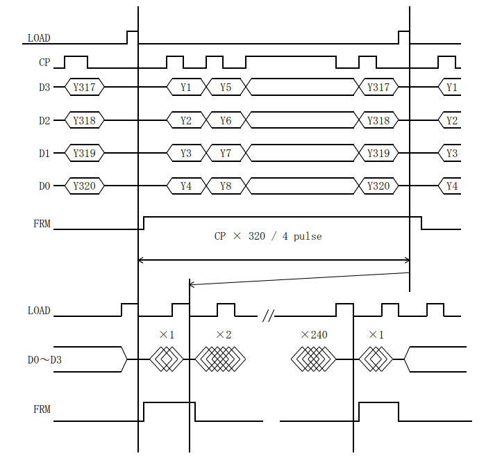
The waveform diagram below was referenced from a similar Kyocera display module.
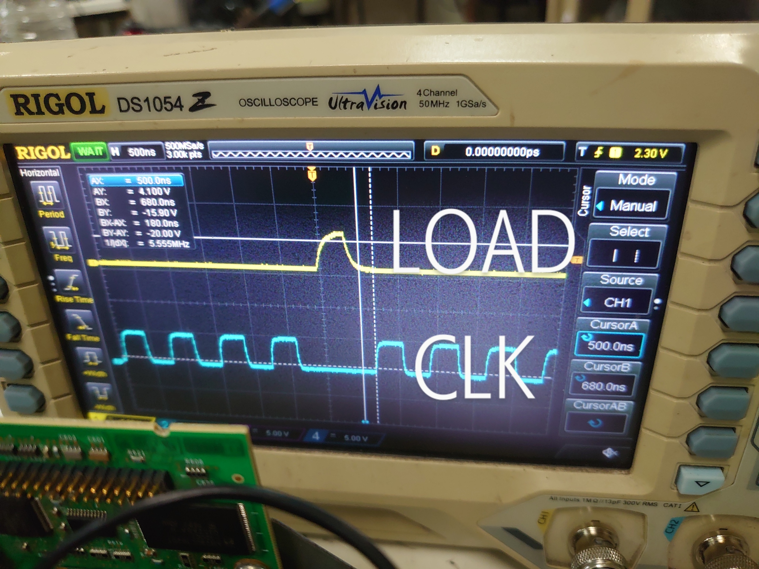
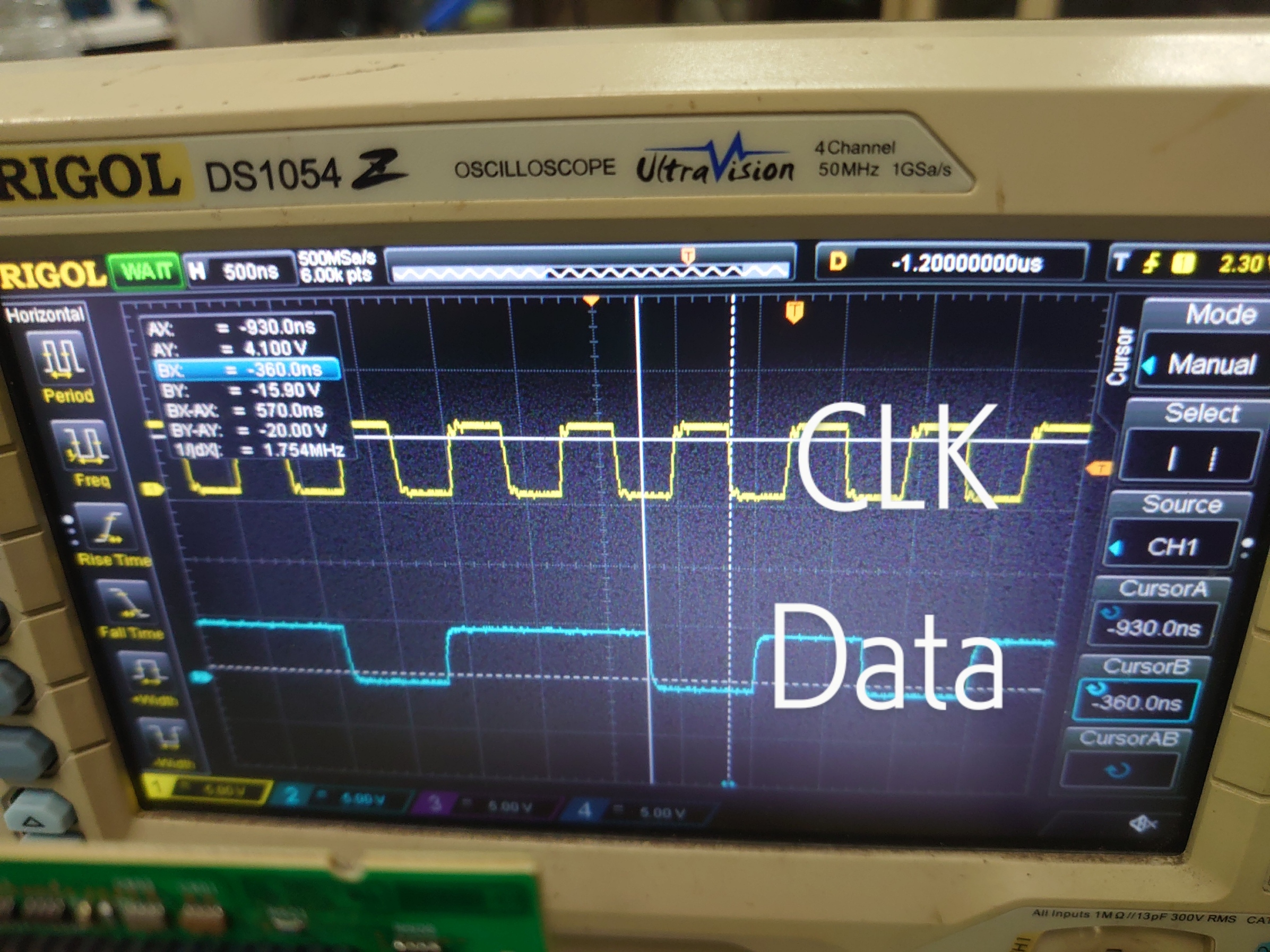
I confirmed this waveform format by probing the signal coming from the ASIC of the TDS1012
 correct
 incorrect