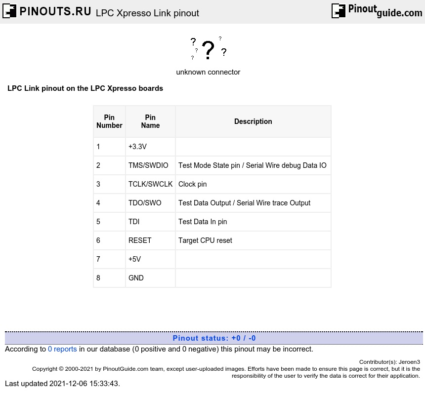
LPC Link pinout on the LPC Xpresso boards.
Pin number 1 is the TOP pair with the USB connector to your LEFT.
| Pin Number |
Pin Name |
Description |
|---|---|---|
| 1 | +3.3V | |
| 2 | TMS/SWDIO | Test Mode State pin / Serial Wire debug Data IO |
| 3 | TCLK/SWCLK | Clock pin |
| 4 | TDO/SWO | Test Data Output / Serial Wire trace Output |
| 5 | TDI | Test Data In pin |
| 6 | RESET | Target CPU reset |
| 7 | +5V | |
| 8 | GND |
See also: ARM JTAG or ARM SWD


 correct
 incorrect