The M.2 standard is designed as a revision and improvement to the mSATA standard, which uses the PCI Express Mini Card physical layout. While mSATA took advantage of the existing PCI Express Mini Card form factor and connector, M.2 has been designed to maximize usage of the card space. Supported host controller interfaces and internally provided ports are a superset to those defined by the SATA Express interface.
The M.2 specification covers multiple Host Interface solutions including:
- PCI Express (PCIe)
- Serial Peripheral Interface (SPI)
- High-Speed Inter-Chip (HSIC)
- SuperSpeed Inter-Chip (SSIC)
- Mobile PCIe (M-PCIe)
- Universal Serial Bus (USB)
- Secure Digital Input Output (SDIO)
- Universal Asynchronous Receiver/Transmitter (UART)
- Pulse Code Modulation / Inter-IC Sound (PCM/I2S)
- Inter-Integrated Circuit (I2C)
- System Management Bus (SMBus)
- Serial ATA (SATA)
- DisplayPort (DP)
- All future variants of the interfaces in this list
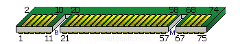
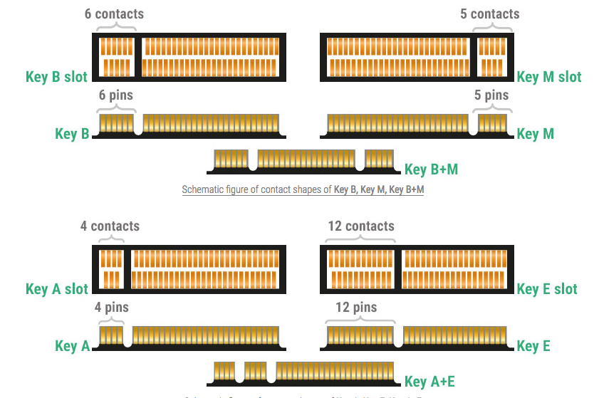
Computer bus interfaces provided through the M.2 connector are PCI Express 3.0 (up to four lanes), Serial ATA 3.0, and USB 3.0 (a single logical port for each of the latter two). It is up to the manufacturer of the M.2 host or device to select which interfaces are to be supported, depending on the desired level of host support and device type. The M.2 connector has different keying notches that denote various purposes and capabilities of M.2 hosts and modules, preventing plugging of M.2 modules into feature-incompatible host connectors
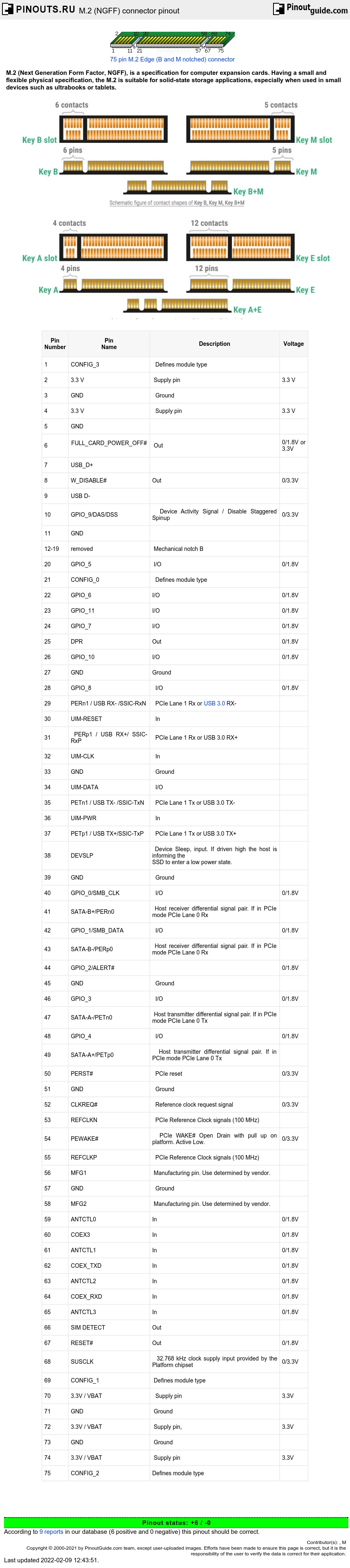
M.2 uses a dual-sided edge card connector with a 0.5 mm contact pitch. There are some mechanical keys defined for SSDs. For example key B M.2 pinout supports SSD/WWAN: 1x SATA SSD or 1x, 2x PCIe SSD (and WWAN) Host Interfaces. Key M M.2 pinout supports SSDs only: 1x SATA or 1x, 2x, or 4x PCIe Host Interfaces. Sockets are defined as follows: Socket 1 accepts cards with an “A” key notch present, Socket 2 accepts cards with a “B” key notch present, Socket 3 accepts cards with an “M” key notch present.
M.2 pinout for key B (1x SATA, 2x PCIe)
| Pin Number |
Pin Name |
Description | Voltage |
|---|---|---|---|
| 1 | CONFIG_3 | Defines module type | |
| 2 | 3.3 V | Supply pin | 3.3 V |
| 3 | GND | Ground | |
| 4 | 3.3 V | Supply pin | 3.3 V |
| 5 | GND | ||
| 6 |
FULL_CARD_POWER_OFF# |
Out | 0/1.8V or 3.3V |
| 7 | USB_D+ | ||
| 8 | W_DISABLE# | Out | 0/3.3V |
| 9 | USB D- | ||
| 10 | GPIO_9/DAS/DSS | Device Activity Signal / Disable Staggered Spinup | 0/3.3V |
| 11 | GND | ||
| 12-19 | removed | Mechanical notch B | |
| 20 | GPIO_5 | I/O | 0/1.8V |
| 21 | CONFIG_0 | Defines module type | |
| 22 | GPIO_6 | I/O | 0/1.8V |
| 23 | GPIO_11 | I/O | 0/1.8V |
| 24 | GPIO_7 | I/O | 0/1.8V |
| 25 | DPR | Out | 0/1.8V |
| 26 | GPIO_10 | I/O | 0/1.8V |
| 27 | GND | Ground | |
| 28 | GPIO_8 | I/O | 0/1.8V |
| 29 | PERn1 / USB RX- /SSIC-RxN | PCIe Lane 1 Rx or USB 3.0 RX- | |
| 30 | UIM-RESET | In | |
| 31 | PERp1 / USB RX+/ SSIC-RxP | PCIe Lane 1 Rx or USB 3.0 RX+ | |
| 32 | UIM-CLK | In | |
| 33 | GND | Ground | |
| 34 | UIM-DATA | I/O | |
| 35 | PETn1 / USB TX- /SSIC-TxN | PCIe Lane 1 Tx or USB 3.0 TX- | |
| 36 | UIM-PWR | In | |
| 37 | PETp1 / USB TX+/SSIC-TxP | PCIe Lane 1 Tx or USB 3.0 TX+ | |
| 38 | DEVSLP | Device Sleep, input. If driven high the host is informing the SSD to enter a low power state. |
|
| 39 | GND | Ground | |
| 40 | GPIO_0/SMB_CLK | I/O | 0/1.8V |
| 41 | SATA-B+/PERn0 | Host receiver differential signal pair. If in PCIe mode PCIe Lane 0 Rx | |
| 42 | GPIO_1/SMB_DATA | I/O | 0/1.8V |
| 43 | SATA-B-/PERp0 | Host receiver differential signal pair. If in PCIe mode PCIe Lane 0 Rx | |
| 44 | GPIO_2/ALERT# | 0/1.8V | |
| 45 | GND | Ground | |
| 46 | GPIO_3 | I/O | 0/1.8V |
| 47 | SATA-A-/PETn0 | Host transmitter differential signal pair. If in PCIe mode PCIe Lane 0 Tx | |
| 48 | GPIO_4 | I/O | 0/1.8V |
| 49 | SATA-A+/PETp0 | Host transmitter differential signal pair. If in PCIe mode PCIe Lane 0 Tx | |
| 50 | PERST# | PCIe reset | 0/3.3V |
| 51 | GND | Ground | |
| 52 | CLKREQ# | Reference clock request signal | 0/3.3V |
| 53 | REFCLKN | PCIe Reference Clock signals (100 MHz) | |
| 54 | PEWAKE# | PCIe WAKE# Open Drain with pull up on platform. Active Low. | 0/3.3V |
| 55 | REFCLKP | PCIe Reference Clock signals (100 MHz) | |
| 56 | MFG1 | Manufacturing pin. Use determined by vendor. | |
| 57 | GND | Ground | |
| 58 | MFG2 | Manufacturing pin. Use determined by vendor. | |
| 59 | ANTCTL0 | In | 0/1.8V |
| 60 | COEX3 | In | 0/1.8V |
| 61 | ANTCTL1 | In | 0/1.8V |
| 62 | COEX_TXD | In | 0/1.8V |
| 63 | ANTCTL2 | In | 0/1.8V |
| 64 | COEX_RXD | In | 0/1.8V |
| 65 | ANTCTL3 | In | 0/1.8V |
| 66 | SIM DETECT | Out | |
| 67 | RESET# | Out | 0/1.8V |
| 68 | SUSCLK | 32.768 kHz clock supply input provided by the Platform chipset | 0/3.3V |
| 69 | CONFIG_1 | Defines module type | |
| 70 | 3.3V / VBAT | Supply pin | 3.3V |
| 71 | GND | Ground | |
| 72 | 3.3V / VBAT | Supply pin, | 3.3V |
| 73 | GND | Ground | |
| 74 | 3.3V / VBAT | Supply pin | 3.3V |
| 75 | CONFIG_2 | Defines module type |
CONFIG pins are set by the SSD to inform the host if the drive wishes to use the SATA or PCIe signaling scheme. SSD-SATA pull pin 1, pin 21, pin 69, pin 75 to Ground.
Config pins configuration:
| Config_0 pin 21 |
Config_1 pin 69 |
Config_2 pin 75 |
Config_3 pin 1 |
Host Interface |
|---|---|---|---|---|
| 0 | 0 | 0 | 0 | SSD-SATA |
| 0 | 1 | 0 | 0 | SSD-PCIe |
| 0 | 0 | 1 | 0 |
WWAN – PCIe (Port Configuration 0) |
| 0 | 1 | 1 | 0 | WWAN – PCIe (Port Configuration 1) |
| 0 | 0 | 0 | 1 |
WWAN – PCIe, USB3.1 Gen1 (Port |
| 0 | 1 | 0 | 1 | WWAN – PCIe, USB3.1 Gen1 (Port Configuration 1) |
| 0 | 0 | 1 | 1 | WWAN – PCIe, USB3.1 Gen1 (Port Configuration 2) |
| 0 | 1 | 1 | 1 | WWAN – PCIe, USB3.1 Gen1 (Port Configuration 3) |
| 1 | 0 | 0 | 0 |
WWAN – SSIC (Port Configuration 0) |
| 1 | 1 | 0 | 0 | WWAN – SSIC (Port Configuration 1) |
| 1 | 0 | 1 | 0 | WWAN – SSIC (Port Configuration 2) |
| 1 | 1 | 1 | 0 | WWAN – SSIC (Port Configuration 3) |
| 1 | 0 | 0 | 1 | WWAN – PCIe (Port Configuration 2) |
| 1 | 1 | 0 | 1 | WWAN – PCIe (Port Configuration 3) |
| 1 | 0 | 1 | 1 | WWAN – PCIe, USB3.1 (vendor defined) |
| 1 | 1 | 1 | 1 | No Add-in card present |
M.2 pinout for key M (1x SATA, 1x, 2x, or 4x PCIe)
| Pin Number |
Pin Name |
Description | Voltage |
|---|---|---|---|
| 1 | CONFIG_3 | Defines module type | |
| 2 | 3.3 V | Supply pin | 3.3 V |
| 3 | GND | Ground | |
| 4 | 3.3 V | Supply pin | 3.3 V |
| 5 | PERn3 | PCIe Lane 3 Rx | |
| 6 | N/A | ||
| 7 | PERp3 | PCIe Lane 3 Rx | |
| 8 | N/A | ||
| 9 | GND | Ground | |
| 10 | DAS/DSS | Device Activity Signal / Disable Staggered Spinup | |
| 11 | PETn3 | PCIe Lane 3 Tx | |
| 12 | 3.3 V | Supply pin | 3.3 V |
| 13 | PETp3 | PCIe Lane 3 Tx | |
| 14 | 3.3 V | Supply pin | 3.3 V |
| 15 | GND | Ground | |
| 16 | 3.3V | Supply pin | 3.3 V |
| 17 | PERn2 | PCIe Lane 2 Rx | |
| 18 | 3.3 V | Supply pin | 3.3 V |
| 19 | PERp2 | PCIe Lane 2 Rx | |
| 20 | N/A | ||
| 21 | CONFIG_0 | Defines module type | |
| 22 | N/A | ||
| 23 | PETn2 | PCIe Lane 2 Tx | |
| 24 | N/A | ||
| 25 | PETp2 | PCIe Lane 2 Tx | |
| 26 | N/A | ||
| 27 | GND | Ground | |
| 28 | N/A | ||
| 29 | PERn1 | PCIe Lane 1 Rx | |
| 30 | N/A | ||
| 31 | PERp1 | PCIe Lane 1 Rx | |
| 32 | N/A | ||
| 33 | GND | Ground | |
| 34 | N/A | ||
| 35 | PETn1 | PCIe Lane 1 Tx | |
| 36 | N/A | ||
| 37 | PETp1 | PCIe Lane 1 Tx | |
| 38 | DEVSLP | Device Sleep, input. If driven high the host is informing the SSD to enter a low power state. |
|
| 39 | GND | Ground | |
| 40 | N/A | ||
| 41 | SATA-B+/PERn0 | Host receiver differential signal pair. If in PCIe mode PCIe Lane 0 Rx | |
| 42 | N/A | ||
| 43 | SATA-B-/PERp0 | Host receiver differential signal pair. If in PCIe mode PCIe Lane 0 Rx | |
| 44 | N/A | ||
| 45 | GND | Ground | |
| 46 | N/A | ||
| 47 | SATA-A-/PETn0 | Host transmitter differential signal pair. If in PCIe mode PCIe Lane 0 Tx | |
| 48 | N/A | ||
| 49 | SATA-A+/PETp0 | Host transmitter differential signal pair. If in PCIe mode PCIe Lane 0 Tx | |
| 50 | PERST# | PCIe reset | |
| 51 | GND | Ground | |
| 52 | CLKREQ# | Reference clock request signal | |
| 53 | REFCLKN | PCIe Reference Clock signals (100 MHz) | |
| 54 | PEWAKE# | PCIe WAKE# Open Drain with pull up on platform. Active Low. | |
| 55 | REFCLKP | PCIe Reference Clock signals (100 MHz) | |
| 56 | MFG1 | Manufacturing pin. Use determined by vendor. | |
| 57 | GND | Ground | |
| 58 | MFG2 | Manufacturing pin. Use determined by vendor. | |
| 59-66 | removed | Mechanical notch M | |
| 67 | N/A | ||
| 68 | SUSCLK | 32.768 kHz clock supply input provided by the Platform chipset | |
| 69 | CONFIG_1 | Defines module type | |
| 70 | 3.3 V | Supply pin | 3.3 V |
| 71 | GND | Ground | |
| 72 | 3.3 V | Supply pin | 3.3 V |
| 73 | GND | Ground | |
| 74 | 3.3 V | Supply pin | 3.3 V |
| 75 | CONFIG_2 | Defines module type |
| Pin id. | Pin name | Description | Voltage |
| 1 | GND | Ground | |
| 2 | +3.3V | power supply | 3.3 V |
| 3 | USB_D+ | USB high-, full-, and low- speed data pair positive | |
| 4 | +3.3V | power supply | 3.3 V |
| 5 | USB_D- | USB high-, full-, and low- speed data pair negative | |
| 6 | LED1# | ||
| 7 | GND | Ground | |
| 8-15 | Key | Substrate removed to act as physical key | |
| 16 | LED2# | ||
| 17 | DNC | Do not connect | |
| 18 | GND | Ground | |
| 19 | DNC | Do not connect | |
| 20 | DNC | Do not connect | |
| 21 | DNC | Do not connect | |
| 22 | DNC | Do not connect | |
| 23-31 | Key | Substrate removed to act as physical key | |
| 32 | DNC | Do not connect | |
| 33 | GND | Ground | |
| 34 | DNC | Do not connect | |
| 35 | PETp0 | PCI Express lane 0 module transmitter pair positive | |
| 36 | DNC | Do not connect | |
| 37 | PETn0 | PCI Express lane 0 module transmitter pair negative | |
| 38 | Vendor defined | ||
| 39 | GND | Ground | |
| 40 | Vendor defined | ||
| 41 | PERp0 | PCI Express lane 0 module receiver pair positive | |
| 42 | Vendor defined | ||
| 43 | PERn0 | PCI Express lane 0 module receiver pair negative | |
| 44 | COEX3 | Antenna coexistence signal 3 | |
| 45 | GND | Ground | |
| 46 | COEX2 | Antenna coexistence signal 2 | |
| 47 | PEFCLKP0 | PCI Express reference clock pair positive | |
| 48 | COEX1 | Antenna coexistence signal 1 | |
| 49 | PEFCLKN0 | PCI Express reference clock pair negative | |
| 50 | SUSCLK | 32.768 kHz clock module input | |
| 51 | GND | Ground | |
| 52 | PERST0# | PCI Express reset | |
| 53 | CLKREQ0# | PCI Express clock request | |
| 54 | W_DISABLE2# | Wireless disable 2 | |
| 55 | PEWake0# | PCI Express wake | |
| 56 | W_DISABLE1# | Wireless disable 1 | |
| 57 | GND | Ground | |
| 58 | SMB_DATA | SMBus data signal | |
| 59 | Reserved | ||
| 60 | SMB_CLK | SMBus clock signal | |
| 61 | Reserved | ||
| 62 | ALERT# | SMBus alert signal | |
| 63 | GND | Ground | |
| 64 | Reserved | ||
| 65 | Reserved | ||
| 66 | UIM_SWP | ||
| 67 | Reserved | ||
| 68 | UIM_POWER_SNK | ||
| 69 | GND | Ground | |
| 70 | UIM_POWER_SRC | ||
| 71 | Reserved | ||
| 72 | +3.3V | power supply | 3.3 V |
| 73 | Reserved | ||
| 74 | +3.3V | power supply | 3.3 V |
| 75 | GND | Ground |
| Pin id. | Pin name | Description | Voltage |
| 1 | GND | Ground | |
| 2 | +3.3V | 3.3 V power supply | |
| 3 | USB_D+ | USB high-, full-, and low- speed data pair positive | |
| 4 | +3.3V | 3.3 V power supply | |
| 5 | USB_D- | USB high-, full-, and low- speed data pair negative | |
| 6 | LED1# | ||
| 7 | GND | Ground | |
| 8 |
PCM_CLK/I2S SCK |
I/O | 0/1.8V |
| 9 | SDIO CLK/SYSCLK | Out | 0/1.8V |
| 10 | PCM SYNC/I2S WS | I/O | 0/1.8V |
| 11 | SDIO CMD | I/O | 0/1.8V |
| 12 | PCM_IN/I2S_IN | In | 0/1.8V |
| 13 | SDIO DATA0 | I/O | 0/1.8V |
| 14 | PCM_OUT/I2S SD_OUT | Out | 0/1.8V |
| 15 | SDIO DATA1 | 0/1.8V | |
| 16 | LED2# | In | |
| 17 | SDIO DATA2 | I/O | 0/1.8V |
| 18 | GND | Ground | |
| 19 | SDIO DATA3 | I/O | 0/1.8V |
| 20 | UART WAKE# | In | 0/3.3V |
| 21 | SDIO WAKE# | In | 0/1.8V |
| 22 | UART RxD | In | 0/1.8V |
| 23 | SDIO RESET#/TX_BLANKING | Out | 0/1.8V |
| 24-31 | Key E | Substrate removed to act as physical key | |
| 32 | UART TxD | Out | 0/1.8V |
| 33 | GND | Ground | |
| 34 | UART CTS | In | 0/1.8V |
| 35 | PETp0 | PCI Express lane 0 module transmitter pair positive | |
| 36 | UART RTS | Out | 0/1.8V |
| 37 | PETn0 | PCI Express lane 0 module transmitter pair negative | |
| 38 | Vendor defined | ||
| 39 | GND | Ground | |
| 40 | Vendor defined | ||
| 41 | PERp0 | PCI Express lane 0 module receiver pair positive | |
| 42 | Vendor defined | ||
| 43 | PERn0 | PCI Express lane 0 module receiver pair negative | |
| 44 | COEX3 | Antenna coexistence signal 3 | 0/1.8V |
| 45 | GND | Ground | |
| 46 | COEX_RxD | In | 0/1.8V |
| 47 | PEFCLKP0 | PCI Express reference clock pair positive | |
| 48 | COEX_TxD | Out | 0/1.8V |
| 49 | PEFCLKN0 | PCI Express reference clock pair negative | |
| 50 | SUSCLK | 32.768 kHz clock module input | 0/3.3V |
| 51 | GND | Ground | |
| 52 | PERST0# | PCI Express reset | 0/3.3V |
| 53 | CLKREQ0# | PCI Express clock request | 0/3.3V |
| 54 | W_DISABLE2# | Wireless disable 2 | 0/3.3V |
| 55 | PEWake0# | PCI Express wake | 0/3.3V |
| 56 | W_DISABLE1# | Wireless disable 1 | 0/3.3V |
| 57 | GND | Ground | |
| 58 | I2C_DATA | I2c data signal | 0/1.8V |
| 59 | Reserved/PETp1 | ||
| 60 | I2c_CLK | I2C clock signal | 0/1.8V |
| 61 | Reserved/PETn1 | ||
| 62 | ALERT# | I2c Bus alert signal In | 0/1.8V |
| 63 | GND | Ground | |
| 64 | Reserved | ||
| 65 | Reserved/PERp1 | ||
| 66 | UIM_SWP/PERST1# | ||
| 67 | Reserved/PERn1 | ||
| 68 | UIM_POWER_SNK/CLKREQ1# | ||
| 69 | GND | Ground | |
| 70 | UIM_POWER_SRC/PEWAKE1# | ||
| 71 | Reserved/REFCLKp1 | ||
| 72 | +3.3V | power supply | 3.3 V |
| 73 | Reserved/REFCLKn1 | ||
| 74 | +3.3V | power supply | 3.3 V |
| 75 | GND | Ground |
M.2 module keying
|
Key |
Pin Location |
Interface |
|---|---|---|
|
A |
8-15 |
2x PCIe x1 / USB 2.0 / I2C /DP x4 |
|
B |
12-19 |
PCIe x2 / SATA /USB 2.0 / USB 3.0 / HSIC / SSIC / Audio / UIM / I2C |
|
C |
16-23 |
Reserved for Future Use |
|
D |
20-27 |
Reserved for Future Use |
|
E |
24-31 |
2x PCIe x1 / USB 2.0 / I2C / SDIO / |
|
F |
28-35 |
Future Memory Interface (FMI) |
|
G |
39-46 |
Not Used for M.2; for Custom/Non-Standard Apps |
|
H |
43-50 |
Reserved for Future Use |
|
J |
47-54 |
Reserved for Future Use |
|
K |
51-58 |
Reserved for Future Use |
|
L |
55-62 |
Reserved for Future Use |
|
M |
59-66 |
PCIe x4 / SATA |
M.2 SATA SSDs are B+M-keyed (can fit in sockets for B-keyed and M-keyed modules), while M.2 NVMe SSDs for PCIe 3.0 x4 lane are M-keyed.
| M.2 key | M.2 module size | M.2 devices |
| A | 1630, 2230, 3030 | WiFi, Bluetooth, NFC and/or WiGig |
| E | 1630, 2230, 3030 | WiFi, Bluetooth, NFC and/or GPS/GNSS |
| B | 3042, 2230, 2242, 2260, 2280, 22110 | 3G/LTE + GPS/GNSS or SSD |
| M | 2242, 2260, 2280, 22110 | SSD with PCIe or SATA interface |
 correct
 incorrect